
1 A Ultra-Low Input Voltage Power Load Switch
Input Voltage Range:VIN: 0.3 V to 5.5 V
Supply voltage range:VBIAS: 1.5 V to 5.5 V
Ultra-Low On-Resistance, RON:30 mΩ Typ. at VIN = 0.3 V, VBIAS = 1.5 V ; 33 mΩ Typ. at VIN = VBIAS = 5.5 V
1.0 A Maximum Continuous Output Current
Quiescent Current, IQ_BIAS:4 µA Typ. at VIN = 0.3 V,VBIAS = 1.5 V ; 5 µA Typ. at VIN = 0.3 V, VBIAS = 5.5 V
Shutdown Current, ISD_BIAS:14 nA Typ. at VBIAS = 3.3 V
Shutdown Current, ISD_VIN:6 nA Typ. at VIN = 5.5 V
Reverse Current Blocking When Disabled
Output Discharge Switch
Operating Temperature Range:- 40°C to + 85°C

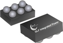
The GLF1591LT is a fully integrated 1 A load switch. The device is ideal for the mobile computing and data storage markets as a high-performance solution for load switch applications.
The GLF1591LT is available in a ultra-thin wafer level chip scale package (WLCSP) measuring 0.67 mm x 1.02 mm x 0.35 mm with a 0.35 mm pitch. This allows the user to save board space.
CPS 0.67 x 1.02 x 0.35


