
Nano Current Consumed Integrated Load Switch with Reset Timer
Ultra-Low ISD:7 nA Typ @ 3.6VBAT
Ultra-Low IQ:3 nA Typ @ 3.6VBAT
Low RON:34mΩ Typ @ 3.6VIN
IOUT Max:2A
Supply Voltage Range:2.5 V to 5.5 V 6 Vabs max
Reset Pulse Period:700 ms
Turn-Off Delay Time:11.6 s
Controlled Output Rise Time:1 ms at 3.6 VBAT
Integrated Output Discharge Switch When Disabled
Operating Temperature Range:-40 to 85 °C
HBM / CDM:6kV / 2kV
Ultra-Small:0.97 mm x 1.47 mm x 0.55mm

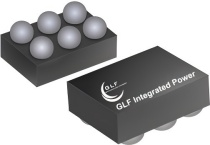
The GLF76121L is an ultra-efficient IQSmartTM load switch with an integrated reset timer for wearables and IoT devices.The GLF7131x features ultra-efficient IQSmartTM technology that supports the lowest quiescent current (IQ) and shutdown current (ISD) in the industry. Low IQ and ISD solutions help designers to reduce parasitic leakage current, improve system efficiency, and increase battery lifetime.
The /SRO pin offers a true reset function enabling the load switch to completely disconnect the load from the input battery after a reasonable long delay time. After the reset period, the main switch of the GLF76121L reconnect the output load to the input battery for normal operation. The GLF76121L has 11.6 second delay time and then 700 ms reset time.
The ultra-low IQ enables direct interface to lower voltage chipset without any external circuit and maintains lower power consumption. The OFF input pin allows the GLF76121L to achieve complete shutdown with total downstream standby current of 7 nA typical. With the switch placed between a battery and system, this switch can help to significantly extend system battery life in mobile devices during shipping or periods of extended off time.
The GLF76121L help to reduce power consumption with the best in class RON and a breakthrough on state IQ of only 3 nA typical when the switch is on.
The GLF76121L integrated 1 ms slew rate control can also enhance system reliability by mitigating bus voltage swings during switching events. Where uncontrolled switching can generate high inrush current that results in voltage droop and/or bus reset events, the GLF slew rate control specifically limits inrush current during turn-on to minimize voltage droop. The output discharge function makes output voltage off quickly during the reset period.
The GLF76121L is available in 0.97 mm x 1.47 mm x 0.55mm wafer level chip scale package (WLCSP).
CSP 0.97 x 1.47 x 0.55


